Empowering Ultra-Pure Sputtering Target Manufacturing Through Custom Automation for KFMI


As a recognized high-tech enterprise and publicly listed company (SZSE: 300666), JFEM has played a pivotal role in eliminating China’s dependence on imported sputtering targets, achieving breakthrough innovations that have earned acceptance by top-tier international chipmakers. Its products are now widely deployed in semiconductor, flat panel display, and solar cell manufacturing sectors across Europe, North America, and Asia.
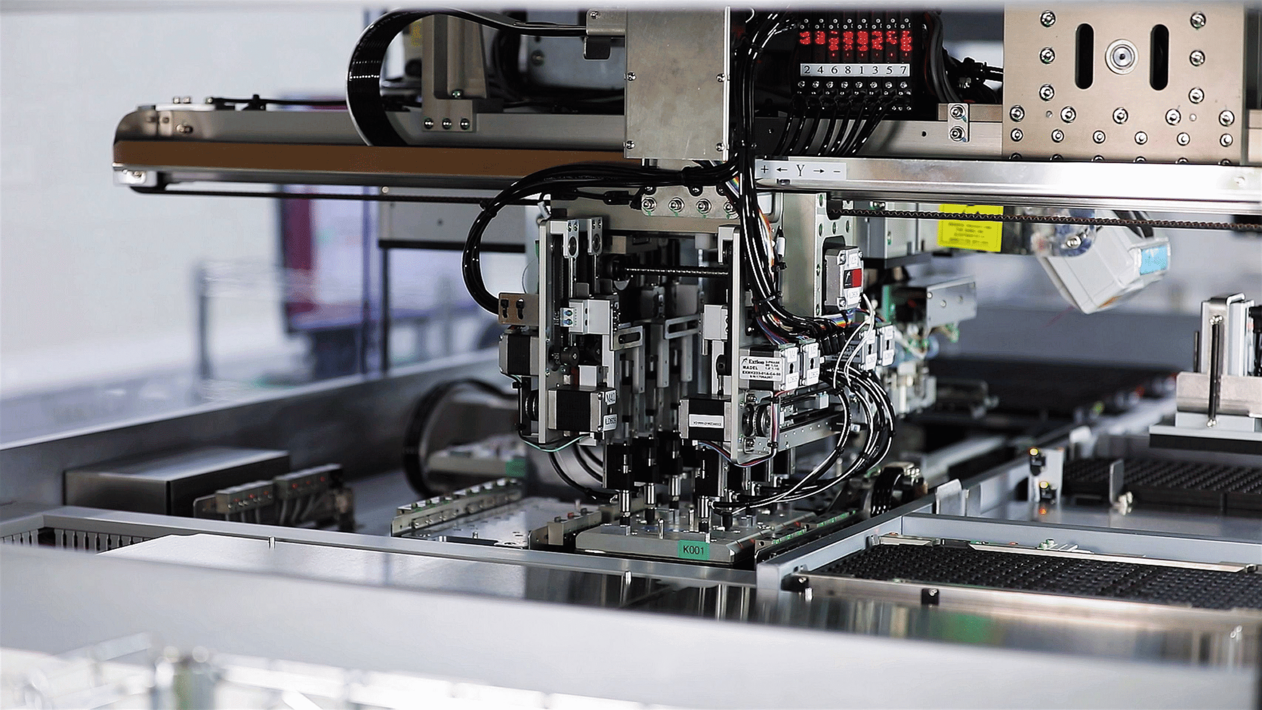
To support JFEM’s growing need for precision, scalability, and material handling efficiency in its complex sputtering target production workflows, Zekta engineered a set of fully customized, high-precision automated systems tailored to the demanding characteristics of high-purity metals such as aluminum, titanium, tantalum, and copper.
Our automation scope included:
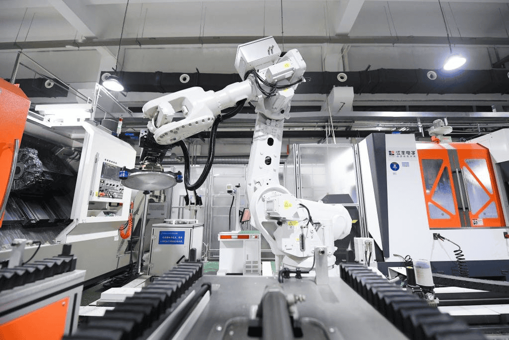
- High-accuracy robotic loading and unloading stations, reducing contamination risk while ensuring the integrity of ultra-pure material surfaces
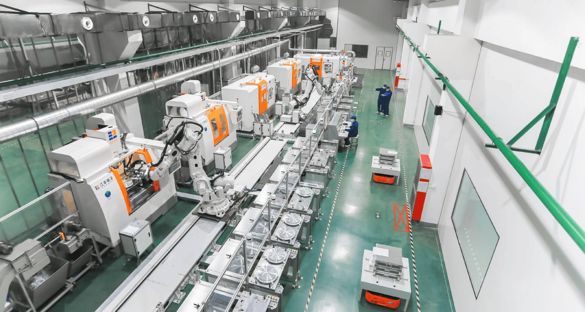
- Modular transfer and inspection platforms, supporting complex handling of large-format target blanks with real-time visual inspection and data capture
- Precision surface treatment modules, designed to meet the micron-level uniformity required for sputtering target bonding and finishing
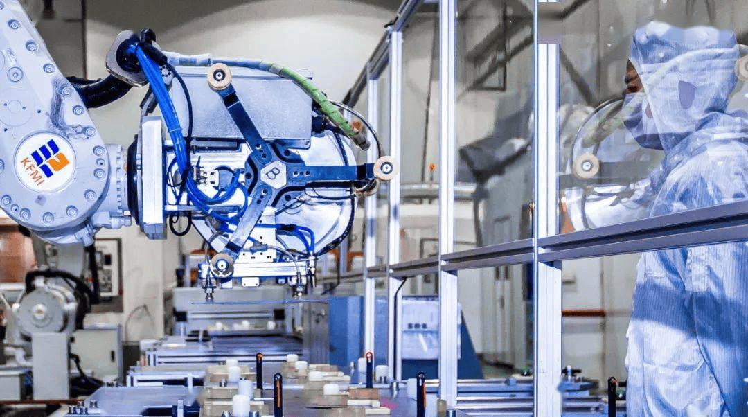
- Cleanroom-compatible automation enclosures, allowing seamless integration into JFEM’s controlled production environments
This automation solution significantly enhanced production repeatability, yield rates, and throughput, while maintaining the stringent purity and dimensional tolerances essential to JFEM’s market-leading sputtering products. It also enabled faster cycle times for newly developed materials entering pilot-scale production, thus accelerating R&D-to-commercialization timelines.
JFEM’s world-class R&D team—comprising returnee PhDs and international experts from the US, Japan, and Singapore—leads the development of cutting-edge processes backed by over 1,000 patent applications, including 90% invention patents. The company has also taken the initiative to establish multiple national and industry standards, making it a true cornerstone of China’s semiconductor materials innovation ecosystem.
This successful collaboration demonstrates how custom intelligent automation can empower top-tier materials manufacturers like JFEM to maintain their technological edge, expand capacity, and better serve the global semiconductor supply chain.
Empowering Ultra-Pure Sputtering Target Manufacturing Through Custom Automation for KFMI
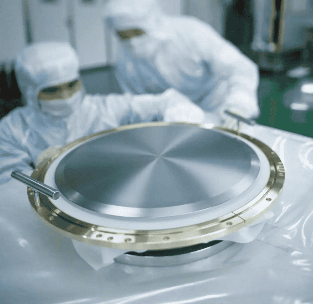
Zekta Automation successfully delivered a bespoke non-standard automation solution to Ningbo Jiangfeng Electronic Materials Co., Ltd. (KFMI), a global leader in the R&D and production of ultra-pure metals and sputtering targetsused in very-large-scale integrated (VLSI) circuit manufacturing.
Performance Showcase of Our Machines